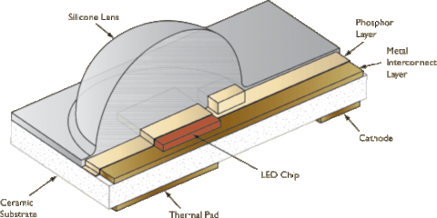
In general, the LED production process has two parts:
Firstly, gallium nitride (GAN) based epitaxial wafers are lining up on the substrate. This process is mainly completed in a metal-organic chemical vapor deposition epitaxial wafer furnace (MOCVD). After preparing the material source and various high-purity gases required for the fabrication of GaN-based epitaxial wafers, the epitaxial wafers can be prepared step by step according to the requirements of the process. Commonly used substrates mainly include sapphire, silicon carbide, and silicon substrates. As well as have GaAs, AlN, ZnO, and other materials.
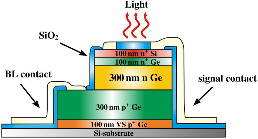
MOCVD uses vapor phase reactants (precursors), group III organic metals, and group V NH3 to react on the substrate surface and deposit the required products on the substrate surface. By controlling temperature, pressure, reactant concentration, and type ratio. And control coating composition and crystal quality. MOCVD epitaxial furnace is the most commonly used equipment for making LED epitaxial wafers.
Then, the two electrodes of the LED PN junction are processed. Electrode processing is also the hinge process of making an LED chip, including cleaning, evaporation, yellow light, chemical etching, fusion, and grinding. Then the required LED chip can be obtained by scribing, testing, and sorting the LED chip. In case the chip cleaning is not clean enough. And the evaporation system is abnormal, and the evaporated metal layer (referring to the electrode after etching) will fall off, the appearance of the metal layer will change color, gold bubbles, and other abnormalities.
During the evaporation process, fixed the chip with a spring clip, so there will be clip marks. Yellow light operation includes baking, photo resisting, photographic exposure, development, etc.

The Manufacturing Process Has 12 Steps
1. LED chip inspection
Microscopic inspection: whether there is mechanical damage on the material surface, whether the size of the lock hill chip and electrode meet the process requirements, and whether the electrode pattern is complete.
2. LED expansion
As the LED chips are still closely arranged after dicing, the spacing is small (about 0.1mm), which is not conducive to the operation of the subsequent process. Use a chip expander to expand the film bonding the chips, make the LED chips draw to 0.6mm. Adopt Manual expansion, but it is easy to cause bad problems such as chip falling and waste.
3. LED dispensing
Apply silver glue or insulating glue at the corresponding position of the LED support. For GaAs and SiC conductive substrates, red light, yellow light, and yellow-green chips with back electrodes use silver glue. For blue and green LED chips with sapphire insulating substrates, use insulating glue to fix the chips.
The processing difficulty lies in the control of dispensing amount. There are detailed process requirements for colloid height and dispensing position.

4. LED glue preparation
Contrary to dispensing, glue preparation uses a glue preparation machine to first apply silver glue on the back electrode of the led, and then install the LED with silver glue on the back of the LED bracket. The efficiency of glue preparation is much higher than that of dispensing, but not all products are suitable for the glue preparation process.
5. LED manual prick
Place the expanded LED chips (with or without glue) on the fixture of the stabbing table, put the LED support under the chucking, and stab the LED chips to the corresponding positions one by one with a needle under the microscope. Compared with automatic rack mounting, manual stabbing has one advantage, which is convenient to replace different chips at any time. It is suitable for products that need to install a variety of chips.
6. LED automatic rack mounting
Automatic rack mounting has two steps: dipping (dispensing) and installing the chip. First, point silver glue (insulating glue) on the LED support, then use the vacuum nozzle to suck the LED chip up to the moving position and place it on the corresponding support position. In the process of automatic rack mounting, it is mainly necessary to be familiar with the operation and programming of the equipment and adjust the glue dipping and installation accuracy of the equipment at the same time. For nozzles to choose from, try to use a bakelite suction nozzle to prevent damage to the surface of the LED chip, especially the blue and green chips must use bakelite. The steel nozzle will scratch the current diffusion layer on the chip surface.
7. LED sintering
The purpose of sintering is to solidify the silver glue. The sintering requires monitoring the temperature to prevent batch defects. The silver glue sintering temperature control at 150 ℃, and the sintering time is 2 hours.
8. LED pressure welding
The purpose of pressure welding is to lead the electrode to the LED chip and complete the connection of internal and external leads of the product. The pressure welding process of LED includes gold wire ball welding and aluminum wire pressure welding.
Pressure welding is a hinge link in LED packaging technology.
9. LED sealant
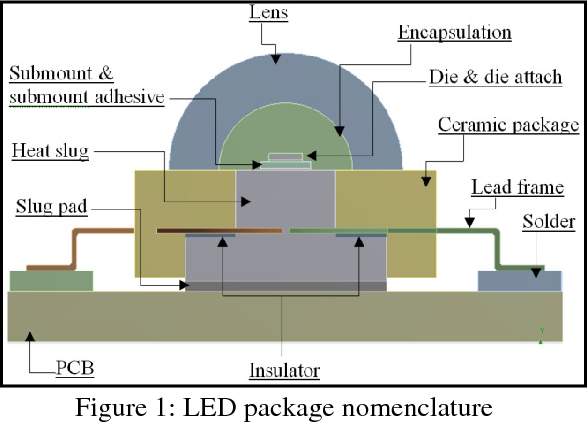
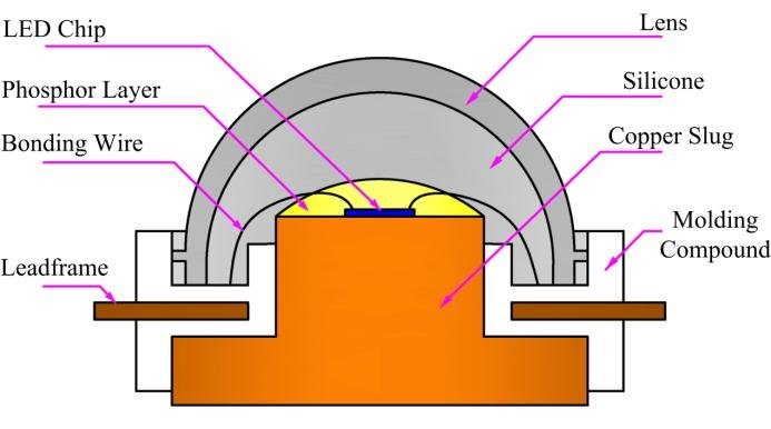
LED packaging mainly includes dispensing, potting, and molding. Difficulties in process control are bubbles, multiple material shortages, and black spots. The design is principal about the selection of materials and the selection of epoxy and brackets with a good combination (General LEDs cannot pass the airtightness test)
Led dispensing top led and side LED are suitable for dispensing packaging. Manual dispensing packaging requires a high operation level (special is white LED). The main difficulty is controlling the dispensing amount because the epoxy will thicken during use. The dispensing of white LED also has the problem of the slight color difference caused by phosphor precipitation. Led glue filling packaging lamp LED is encapsulated in the form of pouring.

10. LED curing and post-curing
Curing refers to the curing of encapsulated epoxy. Generally, the curing condition of epoxy is 135 ℃ for 1 hour. Molded packaging is generally at 150 ℃ for 4 minutes. Post curing is essential to improve the bonding strength between epoxy and support (PCB). The general condition is 120 ℃ for 4 hours.
11. LED rib cutting and scribing
Since LEDs are connected (not single) in production, lamp encapsulated LEDs use rib cutting to cut the connecting rib of LED support. Smd-led is on a PCB board and needs a dicing machine to complete the separation operation.
12. LED test
Test the photoelectric parameters of LED, inspect the overall dimensions, and sort LED products according to customer requirements.
Principal Problems Of An LED chip
The main technical difficulties faced by LED chips, especially high-power LED chips, are mainly in the following aspects:
1. Low luminous efficiency although
The luminous efficiency of packaged white LEDs produced by various manufacturers reaches more than 100lm / W, contrast with small-size LED chips, its luminous efficiency is still very low. A large amount of light is limited inside the device and cannot be emitted, resulting in low light efficiency.
2. Uneven current diffusion
For high-power LED chips, A large current drive needs 350mA. For uniform current spreading, it is necessary to design a reasonable electrode structure to make the current evenly distributed on the p-type layer. Due to the large chip size and the difficulty of uniform diffusion of the current in the p-type layer, the current accumulates below the electrode, causing an electric current crowding effect.
3. Unstable photoelectric characteristics
Due to the low light output efficiency of high-power LED chip devices, the device inside absorbs a large amount of light. This absorbed light is converted into heat energy inside the device, increasing LED chip junction temperature.
4. The light efficiency of industrialization research is far lower than that of laboratory research and development
Although the international mainstream LED chip manufacturers have reached a high level of laboratory research and development, the research level of industrialization is still low.
For more info welcome to visit our company website: www.enetcl.com.

